

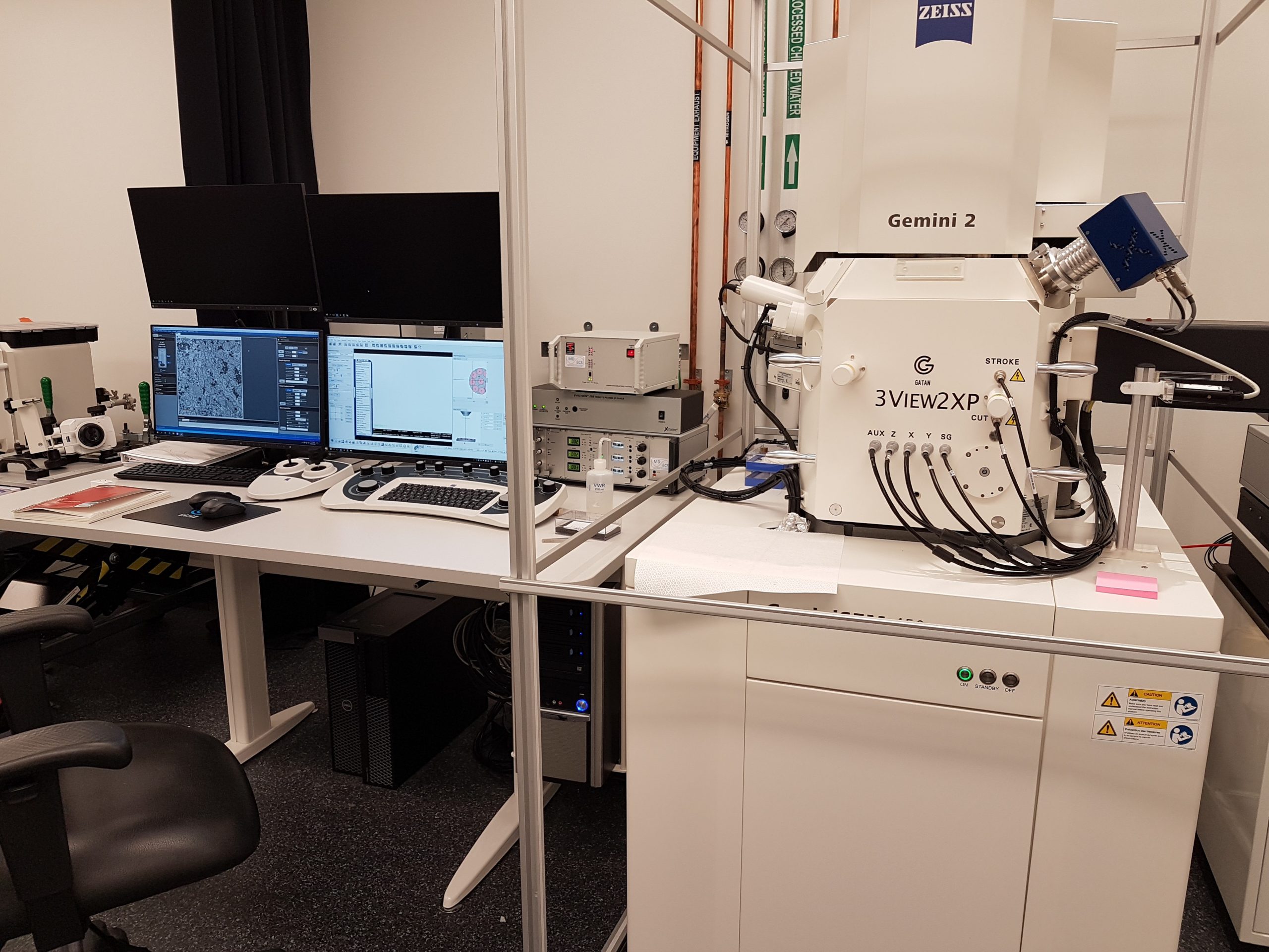
Used scanning electron microscope (SEMs) have evolved into versatile and powerful tools for material characterization, particularly in recent years as the size of materials used in various applications has shrunk.
Electron microscopes image with electrons in the same way that light microscopes do with visible light. Except for transmission electron microscopes (TEMs), which sense electrons that move through a very thin specimen, scanning electron microscopes (SEMs) create images by detecting electrons that are mirrored or knocked off the near-surface region of a sample. Because electrons have a much shorter wavelength than light, SEMs have a higher resolution than light microscopes.
How do SEMs work?
The electron beam scans the sample in a raster pattern in scanning electron microscopy. The electron source first generates electrons at the top of the column. These are emitted when the thermal energy of the source material exceeds the work function of the source material. The positively charged anode then accelerates and attracts them.
The entire electron column must be vacuumed. Like all other components of a used electron microscope for sale, the electron source is sealed inside a special chamber to maintain a vacuum and protect it from contamination, vibrations, and noise. Aside from keeping the electron source clean, a vacuum allows the user to capture a high-resolution image. Other atoms and molecules may be present in the column if there is no vacuum. When they interact with electrons, the electron beam deflects, lowering image quality. The high vacuum also improves the efficiency with which the detectors collect electrons in the column.
Controlling the electron’s path
Lenses, similar to optical transmission electron microscopes, are used to control the path of electrons. Electrons cannot pass through the glass, so the lenses used are electromagnetic. They are simply coils of wire wrapped around metal pole pieces. A magnetic field is created when current flows through the coils. Because electrons are very sensitive to magnetic fields, these electromagnetic lenses can control their path inside the microscope column simply by adjusting the current applied.
Electromagnetic lenses are classified into two types: The condenser lens is the first lens electrons come into contact with as they travel towards the sample. This lens converges the beam before the electron beam cone reopens and is converged again by the objective lens before striking the sample. The condenser lens determines the size of the electron beam (which determines the resolution), whereas the objective lens’s primary function is to focus the beam on the sample.
The lens system of the used transmission electron microscope for sale also includes scanning coils, which are used to raster the beam onto the sample. Apertures are frequently used in conjunction with lenses to control the size of the beam.
Secondary electrons and backscattered electrons
The interaction of electrons within a sample can produce a wide range of electrons, photons, and irradiations. Backscattered (BSE) and secondary electrons are the two types of electrons used for imaging in an SEM (SE).
BSEs are a primary electron beam reflected after elastic interactions between the beam and the sample. On the other hand, secondary electrons come from the sample’s atoms and are the result of inelastic interactions between the electron beam and the sample.
Surface information can be obtained using SE imaging. Because BSEs originate in deeper regions of the sample while SEs originate on the surface, the two carry different types of information. BSE images are highly sensitive to atomic number differences; the higher the atomic number, the brighter the material appears in the image.
Detection of X-rays generated by electron-matter interaction is also widely used in many scanning microscope to perform elemental analysis of the sample. Every material emits X-rays with a specific energy level; X-rays are the material’s fingerprint. It is possible to identify all of the different elements contained in a sample by detecting the energies of X-rays that come out of the sample with an unknown composition.
How are electrons detected?
Different types of detectors detect BSEs and SEs. To maximize BSE collection, solid-state detectors are placed above the sample, concentrically to the electron beam.
The Everhart-Thornley detector is commonly used to detect SEs. It consists of a positively charged scintillator inside a Faraday cage that attracts the SEs. The scintillator is then used to accelerate the electrons and convert them to light before a photomultiplier amplifies them.
The SE detector is angled to the side of the electron to increase the efficiency of detecting SEs, which are then used to form a 3D image of the sample displayed on a PC monitor.
SEM: enchantment but rigor
As you can see, the electrons must go through several processes before an image can be displayed on your monitor. Of course, you don’t have to wait for the electrons to finish their journey; the entire process happens in nanoseconds. At the same time, every “step” of an electron inside the column must be pre-calculated and precisely controlled to produce a high-quality image.